
The progress of PCB assembly started during the twentieth century. In 1903, Albert Hanson who had been a German founder offered a description regarding smooth foil conductors being laminated to an insulating panel in several layers. Also in 1904, Thomas Edison built a test with the substance operations of plating conductors on a linen paper. Furthermore, in 1913, Arthur Berry made a patent of a print-and-etch approach in Britain of which Maximum Schoop obtained a patent in America. It absolutely was also in 1927 that Charles Durcase acquired a patent regarding the technique of electroplating enterprise patterns.
After the PCB is finished, the electrical components should really be attached therefore a functional PCB assembly is formed. You can find two structure processes which can be used to be able to kind the PCB assembly. One could be the through-hole structure in which the part brings are placed in the holes while the other one may be the surface-mount structure when the components are based on pads located on the outside surfaces of the PCB. Equally types of construction have part leads which are repaired mechanically along with electrically to the panel by way of a steel solder 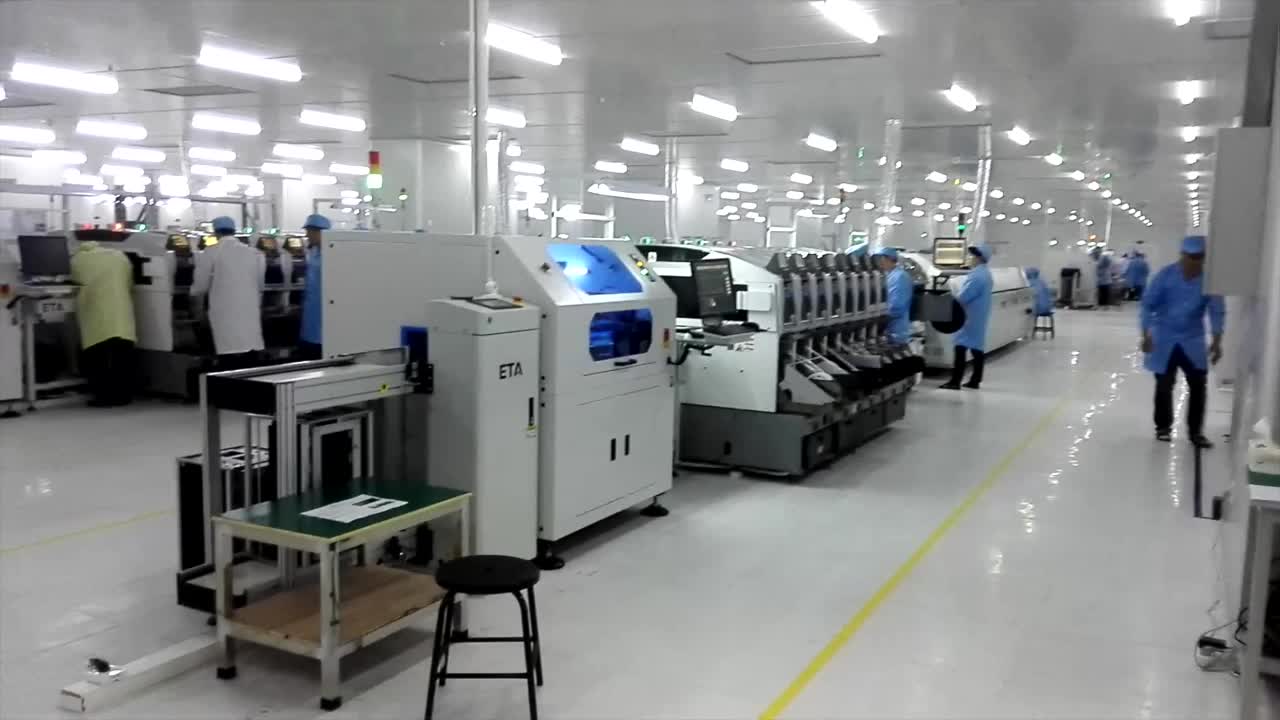 that has melted.
Moreover, there are numerous soldering methods to be properly used to be able to join the PCB components in order that PCB assembly can be possible. Creation that’s of large quantity must be done through unit position and majority trend form of soldering. However, expert specialists have the capacity to solder really minute parts by the give under a microscope. This is often finished with the utilization of tweezers and a soldering metal with an excellent idea which is made for little size prototypes. However, you can find pieces that are difficult to solder with the hands just as the baseball grid array.
The development in engineering nowadays is very fast. You can find therefore several tools which are upgraded every now and then leaving you out from the latest if you do not have the amount of money to find up. It is challenging to acquire a new model right away if your finances don’t let you. You may not have to invest or take debt because of them. This continuous economic disaster should coach you on to be thrifty and to live within your means.
Produced Enterprise Board (PCB) assembly comprises of many electronic parts that allow the functioning of a digital device. PCB assembly services include multi-stage procedures offering putting components on a PCB board, soldering them in position, and checking and testing these components. PCB assembly is usually outsourced by OEMs to a expert organization, as setting up a printed circuit board assembly unit involves a significant investment. You will find countless tiny parts that help total the enterprise in a printed enterprise board.
Having an obsolete computer or unit might make you have an arduous time in correcting its parts. If your device requires a new portion to change the deficiency then finding the sacrifice portion wouldn’t be easy. That brings you to place your unit out and buy a new model. But if you know the very best PCB assembly service you will not need to undergo that process.
Having a PCB assembly service on your own area will definitely stop you far from spending a lot of on the brand new gadgets. A few of the new types are simply current in certain areas. They could match your simple needs but set to waste the technology you will maybe not have the ability to maximize. If you’re contented with the functionality of one’s possessed gadgets then you may not have to get the new models. You could utilize a PCB assembly services service to help you upgrade at less cost. In that case you will simply upgrade the support that you most probably need.
PCB’s which will make up the PCB assembly have conformal layer that is used by means of dipping or spraying after the parts are done soldering. This fur will essentially prevent rust and the dripping of current or possible shorting due to condensation. PCB assembly is static painful and sensitive, thereby; it must be placed inside antistatic bags while it is being transported. Incorrect methods in handling can transfer static charge through the panel and consequently may damage the components.